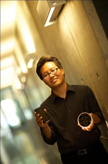
"High Density Chemical Sensor Arrays," by Nosang V. Myung

Electronic detection of molecules is rapidly emerging as an alternative to traditional optical and electrochemical methods because of the small size, low-power consumption, improved sensing performance and, most of all, the possibility of developing high density arrays for simultaneous analyses of multiple species in small sample volumes. Recently, one-dimensional nanostructures (e.g., carbon nanotubes (CNTs), inorganic, and organic nanowires) as conduction channels of field effect transistors (FETs) have been developed for detection of a variety of gaseous and biological molecules with excellent low detection limit, sensitivity, and selectivity. These features are a consequence of dramatic decrease in characteristic length and increase in the ratio of surface to volume atoms, allowing for rapid diffusion into the bulk and for a more significant fraction of the atoms to participate in surface processes such as chemical and biochemical binding interactions. One-dimensional geometries also enhance response times by virtue of their two-dimensional mass transfer profile. Furthermore, nanowires are heralded for device miniaturization and sensor arrays, enabling duplicate elements to reduce false positives/negatives and pattern recognition systems termed electronic noses/tongues where each sensor in the array has a unique response to every analyte creating a fingerprint type response that increases sensitivity and selectivity. Finally, sensors are also attractive for their proven commercial viability, as this approach uses a single material behaving as both the sensitive layer and transducer to directly convert chemical information into an electronic signal without the need for labels, allowing for real-time, continuous monitoring.
In this presentation, synthesis, functionalization, and assembly of various nanoengineered material nanowires will be discussed to create “true” high density gaseous sensor arrays with superior sensing performance in a cost-effective manner. Finally, an Android based smartphone integratable sensor will be demonstrated.
Biography
Professor Nosang Vincent Myung received his B.S. M.S. and Ph. D. Degree in Chemical Engineering from the University of California, Los Angeles in 1994, 1997, and 1998, respectively. He spent three years as a research engineer at the same institution. In 2001-2003 he joined micro electromechanical systems (MEMS) group at Jet Propulsion Laboratory (JPL) as a member of the engineering staff. In 2003 he joined Department of Chemical and Environmental Engineering at University of California, Riverside and served as the Department Chair from 2011-2017.
Currently, he is the founding director for UC-KIMS Center for Innovative Materials for Energy and Environment and co-director for Winston Chung Global Energy Center. During his career he received awards including ECS Electrodeposition Division Research Award, KIChE President Award, Brainpool Fellow from Korean Government, University of California Regent Fellowship, Jet Propulsion Laboratory Spot Award, Abner Brenner gold medal award from American Electroplaters and Surface Finishers Society (AESF), first time author’s award from Plating and Surface Finishing, National Science Foundation graduate fellowship, Department of Education fellowship, American Electroplating and Surface Finishing summer scholarship, and Hughes aircraft company scholarship.
Dr. Myung’s research interests are focused on the synthesis of nanoengineered materials and apply these materials in various advanced applications including spintronics, sensors, electronics, optoelectronics, energy harvesting, and environmental remediation. Dr. Myung’s group objective is to control nanoscale sized features to enhance material properties and device functions beyond those that we currently know. He has had over 200 peer-reviewed journal papers published and his h-index is 53 with the total citation of over 10,000.
Sponsored by the Department of Chemical and Biomolecular Engineering